CN
Home
About CNGE
Susnino Group
CNGE Overview
CNGE developments
Products
Solar wafers
Infrared Optics
Semiconductor
R & D
R & D Overview
R & D Cooperation
R & D Team
R & D BASE
Careers
Careers
Contact Us
Contacts
Leave a Message
中文
Home
>
Products & App
>
Solar wafers
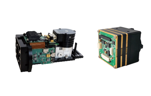
THERMAL IMAGING CORE
Specifications
Application
info@cnge.com.cn cnge.sys@cnge.com.cn
86-25-52752718
No.9 Zhongxing East Road, Lishui Economic Development District, Nanjing, Jiangsu, China
86-25-52752718
info@cnge.com.cn
/ About CNGE
Susnino Group
CNGE Overview
CNGE developments
/ Products
Solar wafers
Infrared Optics
Semiconductor
/ R & D
R & D Overview
R & D Cooperation
R & D Team
R & D BASE
/ Careers
Careers
/ Contact US
Contacts
Leave a Message
CopyRight 2018 中锗科技有限公司版权所有 All rights reserved. 宁ICP备88888888号
技术支持:
35互联